تیم تحریریه جم ترونیک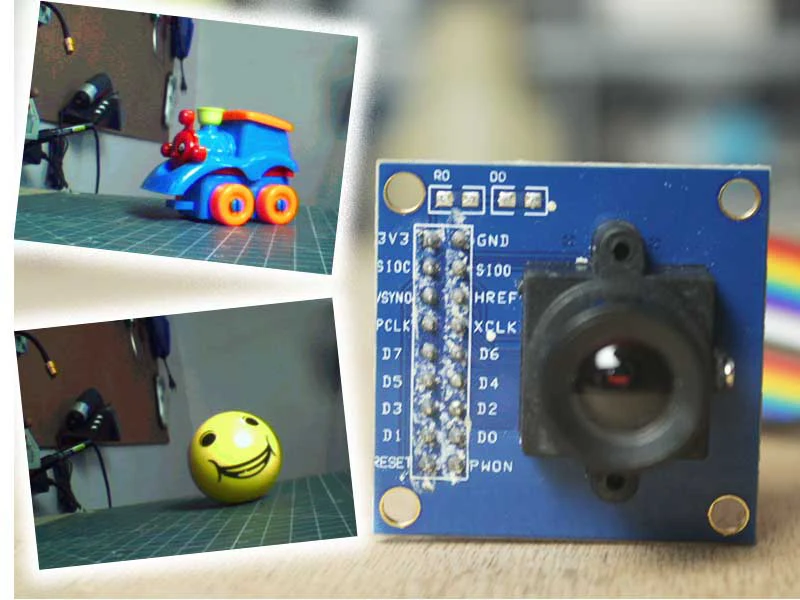
دوربینها به خاطر کاربردهای زیادی که دارند، همواره در صنعت الکترونیک پیشتاز بودهاند. ردپای دوربینها از سادهترین پروژهها تا پیچیدهترین ساختهای الکترونیکی قابل مشاهده است. در این مقاله به بررسی ماژول دوربین OV7670 پرداختهایم؛ سنسوری برای ضبط تصویر و ویدیو با استفاده از آردوینو که در رباتیک، سیستمهای امنیتی و حتی پزشکی کاربرد دارد.
معرفی ماژول دوربین OV7670
این ماژول یک سنسور پردازش تصویر محبوب است که در زمینههای گستردهای از رباتیک تا پزشکی کاربرد دارد؛ ماژول دوربین OV7670 دارای اسیلاتور، تقسیمکننده ولتاژ و قابلیت اتصال به انواع میکروکنترلرها است.
سنسور دوربین OV7670 یک سنسور کممصرف و بهصرفه است که میتواند تصاویر و ویدیوها را با حداکثر رزولوشن ۴۸۰ * ۶۴۰ ضبط کند. این سنسور از پروتکلهای ارتباطی مانند 12C پشتیبانی میکند که باعث میشود این ماژول با سیستمهای مختلفی سازگار باشد.
ماژول دوربین OV7670 دارای سنسور ۰.۳ مگاپیکسلی است و ویدیوهایی با حداکثر ۳۰ فریم بر ثانیه ضبط میکند. این ماژول فقط با ولتاژ ۳.۳ ولت کار میکند، در نتیجه در پروژههای مختلف نباید از پینهای ۵ ولت آردوینو استفاده کنید.
ویژگیهای ماژول دوربین OV7670
- سایز اپتیکال یکششم اینچ
- رزولوشن ۶۴۰ در ۴۸۰
- رگولاتور آنبورد
- عملکرد فقط در ولتاژ ۳.۳ ولت
- لنز شش میلیمتری با کیفیت بالا و F1.8
- حساسیت بالا در مکانهای کمنور
- استفاده از متد واریوپیکسل برای نمونهبرداریهای فرعی
- کنترل تصویر اتوماتیک
- کنترل نوردهی، کنترل Gain، تراز سفیدی اتوماتیک، کالیبراسیون سطح سیاه خودکار
- امکان تنظیم و کنترل کیفیت تصویر شامل Saturation و Sharpness
- ISP شامل کاهش نویز
- پشتیبانی از LED و عکسبرداری با فلش
سختافزار
- سنسور تصویر OV7670: هسته اصلی ماژول دوربین، یک سنسور کممصرف CMOS با عملکرد بالا
- لنز: ماژول دوربین معمولا دارای یک لنز ثابت یا قابل تنظیم است که محدوده دید و کیفیت تصویر را مشخص میکند.
- اسیلاتور: ماژول دوربین OV7670 دارای یک نوسانگر است که کلاک سیگنال را به سنسور تصویر برای افزایش هماهنگی میفرستد.
- رگولاتور ولتاژ: یک تقسیمکننده ولتاژ برای تامین ولتاژهای مختلف ضروری مدار دوربین
- رابط: امکان اتصال به میکروکنترلر را از طریق پروتکلی مانند 12C فراهم میکند.
- مدارهای پشتیبان: این ماژول مدارهای پشتیبانی اضافی مانند خازنهای جداکننده و مقاومتهای پول- آپ
پایهها
- پین VCC: ولتاژ ورودی ۳.۳ ولت
- پین GND
- پین SDIOC: پین 12C سریال کلاک
- پین SDIOD: پین 12C سریال دیتا
- پین VSYNK: هماهنگسازی عمودی تصویر خروجی
- پین HREF: هماهنگسازی افقی تصویر خروجی
- پین XCLK: پین ورودی کلاک سیستم
- پین PCLK: خروجی این پین یک کلاک سیگنال برای هماهنگی انتقال دادههای پیکسل به میکروکنترلر است.
- پینهای D0 تا D7: پینهای انتقال دیتای پیکسل از سنسور به میکروکنترلر
- پین RESET: استفاده برای ریستارت کردن ماژول دوربین
- پین PWDN: پین خاموش کردن ماژول
آموزش راهاندازی ماژول دوربین OV7670
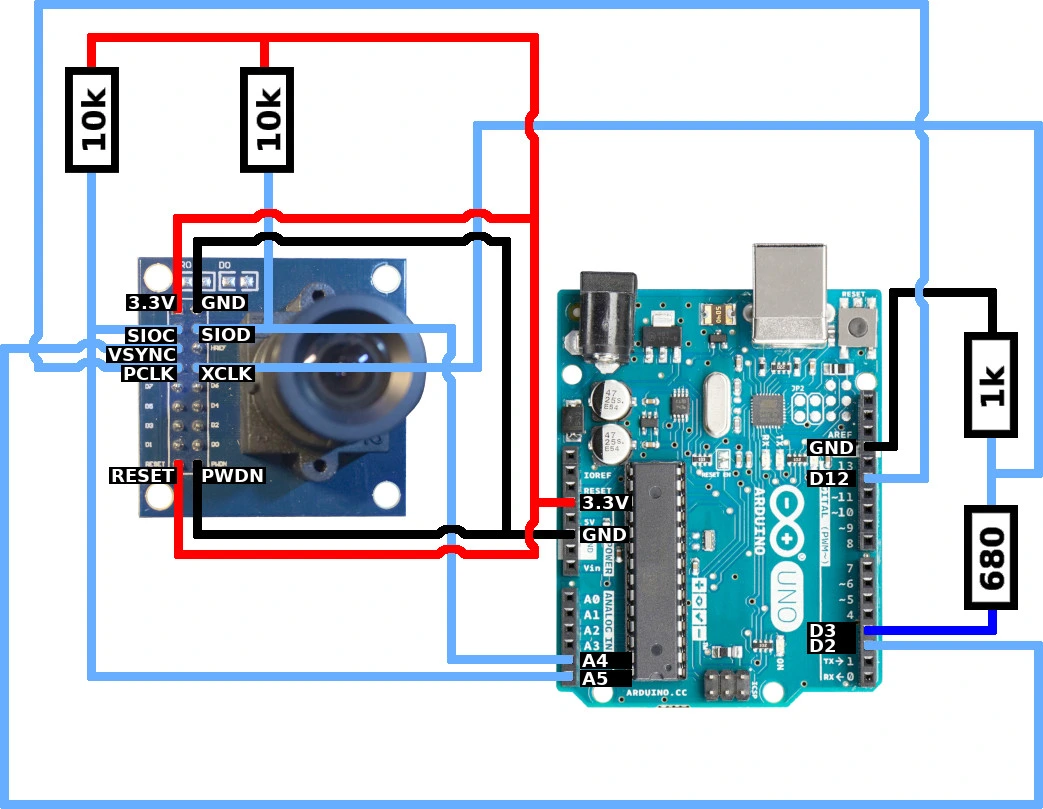
الان که با ماژول دوربین OV7670 آشنا شدهاید، نوبت به راهاندازی آن با آردوینو و استفاده از آن در پروژههای مختلف میرسد. راهاندازی این ممکن است برای افراد مبتدی سختیهایی داشته باشد؛ ما در ادامه این مقاله به سادهترین شکل ممکن راهاندازی این ماژول با استفاده از آردوینو را برایتان فراهم کردهایم.
قطعات مورد نیاز
- آردوینو UNO
- یک USB
- ماژول دوربین OV7670
- دو مقاومت ۱۰ هزار اهم
- دو مقاومت ۴.۷ هزار اهم
- برد بورد
اتصال پایهها
- پین 3v3 را به پین ۳ ولت آردوینو وصل کنید.
- پینهای زمین را به یکدیگر وصل کنید.
- پین SDIOC را به پین A5 آردوینو وصل کنید.
- پین SDIOD را به پین A4 آردوینو متصل کنید.
- پین VSYNK را به پین D3، پین HREF را به پین D8، پین PCLK را به پین D2 و پین XCLK را به پین D11 وصل کنید.
- پینهای D0 تا D3 را به ترتیب به پینهای A0 تا A3 و پینهای D4 تا D7 را به ترتیب به پینهای D4 تا D7 آردوینو وصل کنید.
- پین RESET را به پین 3v3 آردوینو و پین PWDN را به پین GND وصل کنید.
مدارتان را مشابه تصویر بالا بسازید. مقاومتهای ۱۰ هزار اهمی را به شکل موازی به پینهای 3v3 و سیمهای SDIOD و SDIOC متصل کنید. مقاومتهای ۴.۷ هزار اهمی را به پین زمین و پین XCLK اتصال دهید.
برای دریافت تصویر با کیفیت و بدون نویز، سیمهای جامپر را تا حد امکان کوتاه درنظر بگیرید. سیمهای زیاد هم ممکن است باعث اتصال کوتاه مدار شود. از آردوینویی با ولتاژ خروجی ۳.۳ ولت استفاده کنید.
کدنویسی
کدنویسی و راهاندازی ماژول دوربین OV7670 با include کردن کتابخانههای مورد نیاز برای این ماژول در کد آغاز میشود. از آنجایی که این ماژول برپایه پروتکل 12C فعالیت میکند، از کتابخانه <util/twi.h> استفاده میکنیم. تمام این کتابخانهها بهصورت پیشفرض در IDE آردوینو وجود دارند و تنها صدا زدن آنها در کد، کافی است.
تابع setup () شامل تنظیمات اولیه برای گرفتن تصویر است. اولین تابعی که در کد استفاده میکنیم؛
arduinoUnoInut();
است که به آردوینو یک مقدار اولیه میدهد. با این تابع رابطهای ارتباطی مانند PWM Clock، پینهای وقفه، بیتهای برابری و توقف را اضافه میکنیم.
پس از تنظیم آردوینو، نوبت به تنظیم دوربین میرسد. در زمان تنظیم دوربین، تنها امکان تغییر مقدارهای registery وجود دارد؛ این مقدارها را از پیشفرض به مقدار دلخواه خود تغییر میدهیم. همچنین تاخیر مورد نیاز را با توجه به فرکانس میکروکنترلری که استفاده میکنیم، در کد قرار میدهیم. میکروکنترلرهای کندتر، زمان بیشتری برای پردازش صرف کرده و در نتیجه فاصله بین گرفتن تصاویر بیشتر میشود.
void camInit(void){

writeReg(0x12, 0x80);

  _delay_ms(100);

  wrSensorRegs8_8(ov7670_default_regs);

writeReg(REG_COM10, 32);//PCLK does not toggle on HBLANK.

}
دوربین برای گرفتن تصاویر QVGA تنظیم شده است، در نتیجه باید رزولوشن تصاویر را هم تنظیم کنیم. برای این کار از تابع setResolution(); استفاده میکنیم.
با تابع setColor(); میتوان رنگ تصاویر گرفته شده را تعیین کرد. در این آموزش از حالت مونوکروم استفاده شده است؛ مقادیر این تابع بهصورت پیشفرض توسط دوربین تعیین شدهاند و میتوان از بینشان انتخاب نمود.
با استفاده از تابع captureImg(320, 240); میتوان رزولوشن عکس خروجی را تنظیم کرد؛ در این بخش از کد رزولوشن روی ۲۴۰ *۳۲۰ تنظیم شده است.
کد کامل این پروژه در انتهای مقاله قرار گرفته شده است؛ فقط لازم است تا آن را پس از اتصال ماژول به آردوینو، در IDE کپی کنید تا ماژولتان راهاندازی شود.
کد کامل برای راهاندازی ماژول دوربین OV7670
#include <stdint.h>


#include <avr/io.h>


#include <util/twi.h>


#include <util/delay.h>


#include <avr/pgmspace.h>


#define F_CPU 16000000UL


#define vga   0


#define qvga  1


#define qqvga   2


#define yuv422  0


#define rgb565  1


#define bayerRGB  2


#define camAddr_WR  0x42


#define camAddr_RD  0x43


/* Registers */


#define REG_GAIN    0x00  /* Gain lower 8 bits (rest in vref) */


#define REG_BLUE    0x01  /* blue gain */


#define REG_RED       0x02  /* red gain */


#define REG_VREF    0x03  /* Pieces of GAIN, VSTART, VSTOP */


#define REG_COM1    0x04  /* Control 1 */


#define COM1_CCIR656  0x40    /* CCIR656 enable */


#define REG_BAVE    0x05  /* U/B Average level */


#define REG_GbAVE   0x06  /* Y/Gb Average level */


#define REG_AECHH   0x07  /* AEC MS 5 bits */


#define REG_RAVE    0x08  /* V/R Average level */


#define REG_COM2    0x09  /* Control 2 */


#define COM2_SSLEEP         0x10  /* Soft sleep mode */


#define REG_PID           0x0a  /* Product ID MSB */


#define REG_VER           0x0b  /* Product ID LSB */


#define REG_COM3    0x0c  /* Control 3 */


#define COM3_SWAP         0x40  /* Byte swap */


#define COM3_SCALEEN          0x08  /* Enable scaling */


#define COM3_DCWEN          0x04  /* Enable downsamp/crop/window */


#define REG_COM4    0x0d  /* Control 4 */


#define REG_COM5    0x0e  /* All "reserved" */


#define REG_COM6    0x0f  /* Control 6 */


#define REG_AECH    0x10  /* More bits of AEC value */


#define REG_CLKRC   0x11  /* Clocl control */


#define CLK_EXT           0x40  /* Use external clock directly */


#define CLK_SCALE   0x3f  /* Mask for internal clock scale */


#define REG_COM7    0x12  /* Control 7 */ //REG mean address.


#define COM7_RESET          0x80  /* Register reset */


#define COM7_FMT_MASK         0x38


#define COM7_FMT_VGA          0x00


#define COM7_FMT_CIF          0x20  /* CIF format */


#define COM7_FMT_QVGA         0x10  /* QVGA format */


#define COM7_FMT_QCIF         0x08  /* QCIF format */


#define COM7_RGB          0x04  /* bits 0 and 2 - RGB format */


#define COM7_YUV          0x00  /* YUV */


#define COM7_BAYER          0x01  /* Bayer format */


#define COM7_PBAYER         0x05  /* "Processed bayer" */


#define REG_COM8    0x13  /* Control 8 */


#define COM8_FASTAEC          0x80  /* Enable fast AGC/AEC */


#define COM8_AECSTEP          0x40  /* Unlimited AEC step size */


#define COM8_BFILT    0x20  /* Band filter enable */


#define COM8_AGC    0x04  /* Auto gain enable */


#define COM8_AWB    0x02  /* White balance enable */


#define COM8_AEC    0x01  /* Auto exposure enable */


#define REG_COM9    0x14  /* Control 9- gain ceiling */


#define REG_COM10   0x15  /* Control 10 */


#define COM10_HSYNC         0x40  /* HSYNC instead of HREF */


#define COM10_PCLK_HB         0x20  /* Suppress PCLK on horiz blank */


#define COM10_HREF_REV          0x08  /* Reverse HREF */


#define COM10_VS_LEAD         0x04  /* VSYNC on clock leading edge */


#define COM10_VS_NEG          0x02  /* VSYNC negative */


#define COM10_HS_NEG          0x01  /* HSYNC negative */


#define REG_HSTART    0x17  /* Horiz start high bits */


#define REG_HSTOP   0x18  /* Horiz stop high bits */


#define REG_VSTART    0x19  /* Vert start high bits */


#define REG_VSTOP   0x1a  /* Vert stop high bits */


#define REG_PSHFT   0x1b  /* Pixel delay after HREF */


#define REG_MIDH    0x1c  /* Manuf. ID high */


#define REG_MIDL    0x1d  /* Manuf. ID low */


#define REG_MVFP    0x1e  /* Mirror / vflip */


#define MVFP_MIRROR         0x20  /* Mirror image */


#define MVFP_FLIP   0x10  /* Vertical flip */


#define REG_AEW           0x24  /* AGC upper limit */


#define REG_AEB           0x25    /* AGC lower limit */


#define REG_VPT           0x26  /* AGC/AEC fast mode op region */


#define REG_HSYST   0x30  /* HSYNC rising edge delay */


#define REG_HSYEN   0x31  /* HSYNC falling edge delay */


#define REG_HREF    0x32  /* HREF pieces */


#define REG_TSLB    0x3a  /* lots of stuff */


#define TSLB_YLAST    0x04  /* UYVY or VYUY - see com13 */


#define REG_COM11   0x3b  /* Control 11 */


#define COM11_NIGHT         0x80  /* NIght mode enable */


#define COM11_NMFR          0x60  /* Two bit NM frame rate */


#define COM11_HZAUTO          0x10  /* Auto detect 50/60 Hz */


#define COM11_50HZ          0x08  /* Manual 50Hz select */


#define COM11_EXP   0x02


#define REG_COM12   0x3c  /* Control 12 */


#define COM12_HREF          0x80  /* HREF always */


#define REG_COM13   0x3d  /* Control 13 */


#define COM13_GAMMA         0x80  /* Gamma enable */


#define COM13_UVSAT         0x40  /* UV saturation auto adjustment */


#define COM13_UVSWAP          0x01  /* V before U - w/TSLB */


#define REG_COM14   0x3e  /* Control 14 */


#define COM14_DCWEN         0x10  /* DCW/PCLK-scale enable */


#define REG_EDGE    0x3f  /* Edge enhancement factor */


#define REG_COM15   0x40  /* Control 15 */


#define COM15_R10F0         0x00  /* Data range 10 to F0 */


#define COM15_R01FE         0x80  /*      01 to FE */


#define COM15_R00FF         0xc0  /*      00 to FF */


#define COM15_RGB565          0x10  /* RGB565 output */


#define COM15_RGB555          0x30  /* RGB555 output */


#define REG_COM16   0x41  /* Control 16 */


#define COM16_AWBGAIN         0x08  /* AWB gain enable */


#define REG_COM17   0x42  /* Control 17 */


#define COM17_AECWIN          0xc0  /* AEC window - must match COM4 */


#define COM17_CBAR          0x08  /* DSP Color bar */


/*


* This matrix defines how the colors are generated, must be


* tweaked to adjust hue and saturation.


*


* Order: v-red, v-green, v-blue, u-red, u-green, u-blue


* They are nine-bit signed quantities, with the sign bit


* stored in0x58.Sign for v-red is bit 0, and up from there.


*/


#define REG_CMATRIX_BASE  0x4f


#define CMATRIX_LEN           6


#define REG_CMATRIX_SIGN  0x58


#define REG_BRIGHT    0x55  /* Brightness */


#define REG_CONTRAS         0x56  /* Contrast control */


#define REG_GFIX    0x69  /* Fix gain control */


#define REG_REG76   0x76  /* OV's name */


#define R76_BLKPCOR         0x80  /* Black pixel correction enable */


#define R76_WHTPCOR         0x40  /* White pixel correction enable */


#define REG_RGB444          0x8c  /* RGB 444 control */


#define R444_ENABLE         0x02  /* Turn on RGB444, overrides 5x5 */


#define R444_RGBX   0x01  /* Empty nibble at end */


#define REG_HAECC1    0x9f  /* Hist AEC/AGC control 1 */


#define REG_HAECC2    0xa0  /* Hist AEC/AGC control 2 */


#define REG_BD50MAX         0xa5  /* 50hz banding step limit */


#define REG_HAECC3    0xa6  /* Hist AEC/AGC control 3 */


#define REG_HAECC4    0xa7  /* Hist AEC/AGC control 4 */


#define REG_HAECC5    0xa8  /* Hist AEC/AGC control 5 */


#define REG_HAECC6    0xa9  /* Hist AEC/AGC control 6 */


#define REG_HAECC7    0xaa  /* Hist AEC/AGC control 7 */


#define REG_BD60MAX         0xab  /* 60hz banding step limit */


#define REG_GAIN    0x00  /* Gain lower 8 bits (rest in vref) */


#define REG_BLUE    0x01  /* blue gain */


#define REG_RED           0x02  /* red gain */


#define REG_VREF    0x03  /* Pieces of GAIN, VSTART, VSTOP */


#define REG_COM1    0x04  /* Control 1 */


#define COM1_CCIR656          0x40  /* CCIR656 enable */


#define REG_BAVE    0x05  /* U/B Average level */


#define REG_GbAVE   0x06  /* Y/Gb Average level */


#define REG_AECHH   0x07  /* AEC MS 5 bits */


#define REG_RAVE    0x08  /* V/R Average level */


#define REG_COM2    0x09  /* Control 2 */


#define COM2_SSLEEP         0x10  /* Soft sleep mode */


#define REG_PID           0x0a  /* Product ID MSB */


#define REG_VER           0x0b  /* Product ID LSB */


#define REG_COM3    0x0c  /* Control 3 */


#define COM3_SWAP         0x40  /* Byte swap */


#define COM3_SCALEEN          0x08  /* Enable scaling */


#define COM3_DCWEN          0x04  /* Enable downsamp/crop/window */


#define REG_COM4    0x0d  /* Control 4 */


#define REG_COM5    0x0e  /* All "reserved" */


#define REG_COM6    0x0f  /* Control 6 */


#define REG_AECH    0x10  /* More bits of AEC value */


#define REG_CLKRC   0x11  /* Clocl control */


#define CLK_EXT           0x40  /* Use external clock directly */


#define CLK_SCALE   0x3f  /* Mask for internal clock scale */


#define REG_COM7    0x12  /* Control 7 */


#define COM7_RESET          0x80  /* Register reset */


#define COM7_FMT_MASK         0x38


#define COM7_FMT_VGA          0x00


#define COM7_FMT_CIF          0x20  /* CIF format */


#define COM7_FMT_QVGA         0x10  /* QVGA format */


#define COM7_FMT_QCIF         0x08  /* QCIF format */


#define COM7_RGB    0x04  /* bits 0 and 2 - RGB format */


#define COM7_YUV    0x00  /* YUV */


#define COM7_BAYER          0x01  /* Bayer format */


#define COM7_PBAYER         0x05  /* "Processed bayer" */


#define REG_COM8    0x13  /* Control 8 */


#define COM8_FASTAEC          0x80  /* Enable fast AGC/AEC */


#define COM8_AECSTEP          0x40  /* Unlimited AEC step size */


#define COM8_BFILT    0x20  /* Band filter enable */


#define COM8_AGC    0x04  /* Auto gain enable */


#define COM8_AWB    0x02  /* White balance enable */


#define COM8_AEC    0x01  /* Auto exposure enable */


#define REG_COM9    0x14  /* Control 9- gain ceiling */


#define REG_COM10   0x15  /* Control 10 */


#define COM10_HSYNC         0x40  /* HSYNC instead of HREF */


#define COM10_PCLK_HB         0x20  /* Suppress PCLK on horiz blank */


#define COM10_HREF_REV          0x08  /* Reverse HREF */


#define COM10_VS_LEAD           0x04  /* VSYNC on clock leading edge */


#define COM10_VS_NEG          0x02  /* VSYNC negative */


#define COM10_HS_NEG          0x01  /* HSYNC negative */


#define REG_HSTART    0x17  /* Horiz start high bits */


#define REG_HSTOP   0x18  /* Horiz stop high bits */


#define REG_VSTART    0x19  /* Vert start high bits */


#define REG_VSTOP   0x1a  /* Vert stop high bits */


#define REG_PSHFT   0x1b  /* Pixel delay after HREF */


#define REG_MIDH    0x1c  /* Manuf. ID high */


#define REG_MIDL    0x1d  /* Manuf. ID low */


#define REG_MVFP    0x1e  /* Mirror / vflip */


#define MVFP_MIRROR         0x20  /* Mirror image */


#define MVFP_FLIP   0x10  /* Vertical flip */


#define REG_AEW           0x24  /* AGC upper limit */


#define REG_AEB           0x25  /* AGC lower limit */


#define REG_VPT           0x26  /* AGC/AEC fast mode op region */


#define REG_HSYST   0x30  /* HSYNC rising edge delay */


#define REG_HSYEN   0x31  /* HSYNC falling edge delay */


#define REG_HREF    0x32  /* HREF pieces */


#define REG_TSLB    0x3a  /* lots of stuff */


#define TSLB_YLAST    0x04  /* UYVY or VYUY - see com13 */


#define REG_COM11   0x3b  /* Control 11 */


#define COM11_NIGHT         0x80  /* NIght mode enable */


#define COM11_NMFR          0x60  /* Two bit NM frame rate */


#define COM11_HZAUTO          0x10  /* Auto detect 50/60 Hz */


#define COM11_50HZ          0x08  /* Manual 50Hz select */


#define COM11_EXP   0x02


#define REG_COM12   0x3c  /* Control 12 */


#define COM12_HREF          0x80  /* HREF always */


#define REG_COM13   0x3d  /* Control 13 */


#define COM13_GAMMA         0x80  /* Gamma enable */


#define COM13_UVSAT         0x40  /* UV saturation auto adjustment */


#define COM13_UVSWAP          0x01  /* V before U - w/TSLB */


#define REG_COM14   0x3e  /* Control 14 */


#define COM14_DCWEN         0x10  /* DCW/PCLK-scale enable */


#define REG_EDGE    0x3f  /* Edge enhancement factor */


#define REG_COM15   0x40  /* Control 15 */


#define COM15_R10F0         0x00  /* Data range 10 to F0 */


#define COM15_R01FE         0x80  /*      01 to FE */


#define COM15_R00FF         0xc0  /*      00 to FF */


#define COM15_RGB565          0x10  /* RGB565 output */


#define COM15_RGB555          0x30  /* RGB555 output */


#define REG_COM16   0x41  /* Control 16 */


#define COM16_AWBGAIN         0x08  /* AWB gain enable */


#define REG_COM17   0x42  /* Control 17 */


#define COM17_AECWIN          0xc0  /* AEC window - must match COM4 */


#define COM17_CBAR          0x08  /* DSP Color bar */


#define CMATRIX_LEN             6


#define REG_BRIGHT    0x55  /* Brightness */


#define REG_REG76   0x76  /* OV's name */


#define R76_BLKPCOR         0x80  /* Black pixel correction enable */


#define R76_WHTPCOR         0x40  /* White pixel correction enable */


#define REG_RGB444          0x8c  /* RGB 444 control */


#define R444_ENABLE         0x02  /* Turn on RGB444, overrides 5x5 */


#define R444_RGBX   0x01  /* Empty nibble at end */


#define REG_HAECC1    0x9f  /* Hist AEC/AGC control 1 */


#define REG_HAECC2    0xa0  /* Hist AEC/AGC control 2 */


#define REG_BD50MAX         0xa5  /* 50hz banding step limit */


#define REG_HAECC3    0xa6  /* Hist AEC/AGC control 3 */


#define REG_HAECC4    0xa7  /* Hist AEC/AGC control 4 */


#define REG_HAECC5    0xa8  /* Hist AEC/AGC control 5 */


#define REG_HAECC6    0xa9  /* Hist AEC/AGC control 6 */


#define REG_HAECC7    0xaa  /* Hist AEC/AGC control 7 */


#define REG_BD60MAX         0xab  /* 60hz banding step limit */


#define MTX1            0x4f  /* Matrix Coefficient 1 */


#define MTX2            0x50  /* Matrix Coefficient 2 */


#define MTX3            0x51  /* Matrix Coefficient 3 */


#define MTX4            0x52  /* Matrix Coefficient 4 */


#define MTX5            0x53  /* Matrix Coefficient 5 */


#define MTX6            0x54  /* Matrix Coefficient 6 */


#define REG_CONTRAS         0x56  /* Contrast control */


#define MTXS            0x58  /* Matrix Coefficient Sign */


#define AWBC7           0x59  /* AWB Control 7 */


#define AWBC8           0x5a  /* AWB Control 8 */


#define AWBC9           0x5b  /* AWB Control 9 */


#define AWBC10            0x5c  /* AWB Control 10 */


#define AWBC11            0x5d  /* AWB Control 11 */


#define AWBC12            0x5e  /* AWB Control 12 */


#define REG_GFI           0x69  /* Fix gain control */


#define GGAIN           0x6a  /* G Channel AWB Gain */


#define DBLV            0x6b


#define AWBCTR3           0x6c  /* AWB Control 3 */


#define AWBCTR2           0x6d  /* AWB Control 2 */


#define AWBCTR1           0x6e  /* AWB Control 1 */


#define AWBCTR0           0x6f  /* AWB Control 0 */


struct regval_list{


  uint8_t reg_num;


  uint16_t value;


};


const struct regval_list qvga_ov7670[] PROGMEM = {


  { REG_COM14, 0x19 },


  { 0x72, 0x11 },


  { 0x73, 0xf1 },


  { REG_HSTART, 0x16 },


  { REG_HSTOP, 0x04 },


  { REG_HREF, 0xa4 },


  { REG_VSTART, 0x02 },


  { REG_VSTOP, 0x7a },


  { REG_VREF, 0x0a },


  { 0xff, 0xff }, /* END MARKER */


};


const struct regval_list yuv422_ov7670[] PROGMEM = {


  { REG_COM7, 0x0 },  /* Selects YUV mode */


  { REG_RGB444, 0 },  /* No RGB444 please */


  { REG_COM1, 0 },


  { REG_COM15, COM15_R00FF },


  { REG_COM9, 0x6A }, /* 128x gain ceiling; 0x8 is reserved bit */


  { 0x4f, 0x80 },   /* "matrix coefficient 1" */


  { 0x50, 0x80 },   /* "matrix coefficient 2" */


  { 0x51, 0 },    /* vb */


  { 0x52, 0x22 },   /* "matrix coefficient 4" */


  { 0x53, 0x5e },   /* "matrix coefficient 5" */


  { 0x54, 0x80 },   /* "matrix coefficient 6" */


  { REG_COM13, COM13_UVSAT },


  { 0xff, 0xff },   /* END MARKER */


};


const struct regval_list ov7670_default_regs[] PROGMEM = {//from the linux driver


  { REG_COM7, COM7_RESET },


  { REG_TSLB, 0x04 }, /* OV */


  { REG_COM7, 0 },  /* VGA */


  /*


  * Set the hardware window.  These values from OV don't entirely


  * make sense - hstop is less than hstart.  But they work...


  */


  { REG_HSTART, 0x13 }, { REG_HSTOP, 0x01 },


  { REG_HREF, 0xb6 }, { REG_VSTART, 0x02 },


  { REG_VSTOP, 0x7a }, { REG_VREF, 0x0a },


  { REG_COM3, 0 }, { REG_COM14, 0 },


  /* Mystery scaling numbers */


  { 0x70, 0x3a }, { 0x71, 0x35 },


  { 0x72, 0x11 }, { 0x73, 0xf0 },


  { 0xa2,/* 0x02 changed to 1*/1 }, { REG_COM10, 0x0 },


  /* Gamma curve values */


  { 0x7a, 0x20 }, { 0x7b, 0x10 },


  { 0x7c, 0x1e }, { 0x7d, 0x35 },


  { 0x7e, 0x5a }, { 0x7f, 0x69 },


  { 0x80, 0x76 }, { 0x81, 0x80 },


  { 0x82, 0x88 }, { 0x83, 0x8f },


  { 0x84, 0x96 }, { 0x85, 0xa3 },


  { 0x86, 0xaf }, { 0x87, 0xc4 },


  { 0x88, 0xd7 }, { 0x89, 0xe8 },


  /* AGC and AEC parameters.  Note we start by disabling those features,


  then turn them only after tweaking the values. */


  { REG_COM8, COM8_FASTAEC | COM8_AECSTEP },


  { REG_GAIN, 0 }, { REG_AECH, 0 },


  { REG_COM4, 0x40 }, /* magic reserved bit */


  { REG_COM9, 0x18 }, /* 4x gain + magic rsvd bit */


  { REG_BD50MAX, 0x05 }, { REG_BD60MAX, 0x07 },


  { REG_AEW, 0x95 }, { REG_AEB, 0x33 },


  { REG_VPT, 0xe3 }, { REG_HAECC1, 0x78 },


  { REG_HAECC2, 0x68 }, { 0xa1, 0x03 }, /* magic */


  { REG_HAECC3, 0xd8 }, { REG_HAECC4, 0xd8 },


  { REG_HAECC5, 0xf0 }, { REG_HAECC6, 0x90 },


  { REG_HAECC7, 0x94 },


  { REG_COM8, COM8_FASTAEC | COM8_AECSTEP | COM8_AGC | COM8_AEC },


  { 0x30, 0 }, { 0x31, 0 },//disable some delays


  /* Almost all of these are magic "reserved" values.  */


  { REG_COM5, 0x61 }, { REG_COM6, 0x4b },


  { 0x16, 0x02 }, { REG_MVFP, 0x07 },


  { 0x21, 0x02 }, { 0x22, 0x91 },


  { 0x29, 0x07 }, { 0x33, 0x0b },


  { 0x35, 0x0b }, { 0x37, 0x1d },


  { 0x38, 0x71 }, { 0x39, 0x2a },


  { REG_COM12, 0x78 }, { 0x4d, 0x40 },


  { 0x4e, 0x20 }, { REG_GFIX, 0 },


  /*{0x6b, 0x4a},*/{ 0x74, 0x10 },


  { 0x8d, 0x4f }, { 0x8e, 0 },


  { 0x8f, 0 }, { 0x90, 0 },


  { 0x91, 0 }, { 0x96, 0 },


  { 0x9a, 0 }, { 0xb0, 0x84 },


  { 0xb1, 0x0c }, { 0xb2, 0x0e },


  { 0xb3, 0x82 }, { 0xb8, 0x0a },


  /* More reserved magic, some of which tweaks white balance */


  { 0x43, 0x0a }, { 0x44, 0xf0 },


  { 0x45, 0x34 }, { 0x46, 0x58 },


  { 0x47, 0x28 }, { 0x48, 0x3a },


  { 0x59, 0x88 }, { 0x5a, 0x88 },


  { 0x5b, 0x44 }, { 0x5c, 0x67 },


  { 0x5d, 0x49 }, { 0x5e, 0x0e },


  { 0x6c, 0x0a }, { 0x6d, 0x55 },


  { 0x6e, 0x11 }, { 0x6f, 0x9e }, /* it was 0x9F "9e for advance AWB" */


  { 0x6a, 0x40 }, { REG_BLUE, 0x40 },


  { REG_RED, 0x60 },


  { REG_COM8, COM8_FASTAEC | COM8_AECSTEP | COM8_AGC | COM8_AEC | COM8_AWB },


  /* Matrix coefficients */


  { 0x4f, 0x80 }, { 0x50, 0x80 },


  { 0x51, 0 },    { 0x52, 0x22 },


  { 0x53, 0x5e }, { 0x54, 0x80 },


  { 0x58, 0x9e },


  { REG_COM16, COM16_AWBGAIN }, { REG_EDGE, 0 },


  { 0x75, 0x05 }, { REG_REG76, 0xe1 },


  { 0x4c, 0 },     { 0x77, 0x01 },


  { REG_COM13, /*0xc3*/0x48 }, { 0x4b, 0x09 },


  { 0xc9, 0x60 },   /*{REG_COM16, 0x38},*/


  { 0x56, 0x40 },


  { 0x34, 0x11 }, { REG_COM11, COM11_EXP | COM11_HZAUTO },


  { 0xa4, 0x82/*Was 0x88*/ }, { 0x96, 0 },


  { 0x97, 0x30 }, { 0x98, 0x20 },


  { 0x99, 0x30 }, { 0x9a, 0x84 },


  { 0x9b, 0x29 }, { 0x9c, 0x03 },


  { 0x9d, 0x4c }, { 0x9e, 0x3f },


  { 0x78, 0x04 },


  /* Extra-weird stuff.  Some sort of multiplexor register */


  { 0x79, 0x01 }, { 0xc8, 0xf0 },


  { 0x79, 0x0f }, { 0xc8, 0x00 },


  { 0x79, 0x10 }, { 0xc8, 0x7e },


  { 0x79, 0x0a }, { 0xc8, 0x80 },


  { 0x79, 0x0b }, { 0xc8, 0x01 },


  { 0x79, 0x0c }, { 0xc8, 0x0f },


  { 0x79, 0x0d }, { 0xc8, 0x20 },


  { 0x79, 0x09 }, { 0xc8, 0x80 },


  { 0x79, 0x02 }, { 0xc8, 0xc0 },


  { 0x79, 0x03 }, { 0xc8, 0x40 },


  { 0x79, 0x05 }, { 0xc8, 0x30 },


  { 0x79, 0x26 },


  { 0xff, 0xff }, /* END MARKER */


};


void error_led(void){


  DDRB |= 32;//make sure led is output


  while (1){//wait for reset


    PORTB ^= 32;// toggle led


    _delay_ms(100);


  }


}


void twiStart(void){


  TWCR = _BV(TWINT) | _BV(TWSTA) | _BV(TWEN);//send start


  while (!(TWCR & (1 << TWINT)));//wait for start to be transmitted


  if ((TWSR & 0xF8) != TW_START)


    error_led();


}


void twiWriteByte(uint8_t DATA, uint8_t type){


  TWDR = DATA;


  TWCR = _BV(TWINT) | _BV(TWEN);


  while (!(TWCR & (1 << TWINT))) {}


  if ((TWSR & 0xF8) != type)


    error_led();


}


void twiAddr(uint8_t addr, uint8_t typeTWI){


  TWDR = addr;//send address


  TWCR = _BV(TWINT) | _BV(TWEN);    /* clear interrupt to start transmission */


  while ((TWCR & _BV(TWINT)) == 0); /* wait for transmission */


  if ((TWSR & 0xF8) != typeTWI)


    error_led();


}


voidwriteReg(uint8_t reg, uint8_t dat){


  //send start condition


  twiStart();


  twiAddr(camAddr_WR, TW_MT_SLA_ACK);


  twiWriteByte(reg, TW_MT_DATA_ACK);


  twiWriteByte(dat, TW_MT_DATA_ACK);


  TWCR = (1 << TWINT) | (1 << TWEN) | (1 << TWSTO);//send stop


  _delay_ms(1);


}


static uint8_t twiRd(uint8_t nack){


  if (nack){


    TWCR = _BV(TWINT) | _BV(TWEN);


    while ((TWCR & _BV(TWINT)) == 0); /* wait for transmission */


    if ((TWSR & 0xF8) != TW_MR_DATA_NACK)


      error_led();


    return TWDR;


  }


  else{


    TWCR = _BV(TWINT) | _BV(TWEN) | _BV(TWEA);


    while ((TWCR & _BV(TWINT)) == 0); /* wait for transmission */


    if ((TWSR & 0xF8) != TW_MR_DATA_ACK)


      error_led();


    return TWDR;


  }


}


uint8_t rdReg(uint8_t reg){


  uint8_t dat;


  twiStart();


  twiAddr(camAddr_WR, TW_MT_SLA_ACK);


  twiWriteByte(reg, TW_MT_DATA_ACK);


  TWCR = (1 << TWINT) | (1 << TWEN) | (1 << TWSTO);//send stop


  _delay_ms(1);


  twiStart();


  twiAddr(camAddr_RD, TW_MR_SLA_ACK);


  dat = twiRd(1);


  TWCR = (1 << TWINT) | (1 << TWEN) | (1 << TWSTO);//send stop


  _delay_ms(1);


  return dat;


}


void wrSensorRegs8_8(const struct regval_list reglist[]){


  uint8_t reg_addr, reg_val;


  const struct regval_list *next = reglist;


  while ((reg_addr != 0xff) | (reg_val != 0xff)){


    reg_addr = pgm_read_byte(&next->reg_num);


    reg_val = pgm_read_byte(&next->value);


   writeReg(reg_addr, reg_val);


    next++;


  }


}


void setColor(void){


  wrSensorRegs8_8(yuv422_ov7670);


 // wrSensorRegs8_8(qvga_ov7670);


}


void setResolution(void){


 writeReg(REG_COM3, 4); // REG_COM3 enable scaling


  wrSensorRegs8_8(qvga_ov7670);


}


void camInit(void){


 writeReg(0x12, 0x80);


  _delay_ms(100);


  wrSensorRegs8_8(ov7670_default_regs);


 writeReg(REG_COM10, 32);//PCLK does not toggle on HBLANK.


}


void arduinoUnoInut(void) {


  cli();//disable interrupts


    /* Setup the 8mhz PWM clock


  * This will be on pin 11*/


  DDRB |= (1 << 3);//pin 11


  ASSR &= ~(_BV(EXCLK) | _BV(AS2));


  TCCR2A = (1 << COM2A0) | (1 << WGM21) | (1 << WGM20);


  TCCR2B = (1 << WGM22) | (1 << CS20);


  OCR2A = 0;//(F_CPU)/(2*(X+1))


  DDRC &= ~15;//low d0-d3 camera


  DDRD &= ~252;//d7-d4 and interrupt pins


  _delay_ms(3000);


    //set up twi for 100khz


  TWSR &= ~3;//disable prescaler for TWI


  TWBR = 72;//set to 100khz


    //enable serial


  UBRR0H = 0;


  UBRR0L = 1;//0 = 2M baud rate. 1 = 1M baud. 3 = 0.5M. 7 = 250k 207 is 9600 baud rate.


  UCSR0A |= 2;//double speed aysnc


  UCSR0B = (1 << RXEN0) | (1 << TXEN0);//Enable receiver and transmitter


  UCSR0C = 6;//async 1 stop bit 8bit char no parity bits


}


void StringPgm(const char * str){


  do{


      while (!(UCSR0A & (1 << UDRE0)));//wait for byte to transmit


      UDR0 = pgm_read_byte_near(str);


      while (!(UCSR0A & (1 << UDRE0)));//wait for byte to transmit


  } while (pgm_read_byte_near(++str));


}


static void captureImg(uint16_t wg, uint16_t hg){


  uint16_t y, x;


  StringPgm(PSTR("*RDY*"));


  while (!(PIND & 8));//wait for high


  while ((PIND & 8));//wait for low


    y = hg;


  while (y--){


        x = wg;


      //while (!(PIND & 256));//wait for high


    while (x--){


      while ((PIND & 4));//wait for low


            UDR0 = (PINC & 15) | (PIND & 240);


          while (!(UCSR0A & (1 << UDRE0)));//wait for byte to transmit


      while (!(PIND & 4));//wait for high


      while ((PIND & 4));//wait for low


      while (!(PIND & 4));//wait for high


    }


    //  while ((PIND & 256));//wait for low


  }


    _delay_ms(100);


}


void setup(){


  arduinoUnoInut();


  camInit();


  setResolution();


  setColor();


 writeReg(0x11, 10); //Earlier it had the value:writeReg(0x11, 12); New version works better for me :) !!!!


}


void loop(){


  captureImg(320, 240);


}
جمعبندی
ماژول دوربین OV7670 دارای کاربردهای زیادی است و میتوانید از آن در پروژههای مختلفی استفاده کنید. ما در این مقاله این ماژول را بررسی کرده و راهاندازی آن را آموزش دادیم. راهاندازی این ماژول ممکن است برای افراد مبتدی ساده نباشد، به همین دلیل باید دقت بالایی داشته باشید تا به ماژول آسیبی نرسد.